Embedded Electronics

Embedded Electronics with FDM/FFF 3D Printing
Print the structure, conductive pathways and electronics in the same manufacturing workflow.
Kupros is excited to introduce our patent-pending embedded electronics process for FDM/FFF 3D printing.
Using Kupros Cu29 all-metal, conductive filament, engineers can integrate conductive pathways, circuits, sensors, antennas and electronic components directly into or onto 3D printed structures during the manufacturing process.
Instead of printing a polymer part and then adding wiring, circuit boards, sensors and electronic components afterward, the electronics can become part of the printed structure itself.
The result is a new way to manufacture functional electronics using the FDM/FFF equipment engineers already own.
Turn Your 3D Printer Into an Electronics Factory
FDM/FFF printers are traditionally used to manufacture mechanical parts, housings, fixtures and prototypes.
Kupros is extending that same manufacturing platform into electronics.
Our patent-pending process combines:
Structural FDM/FFF materials
Cu29 all-metal conductive pathways
Embedded circuits
Sensors and strain gauges
Antennas and RF structures
Conductive interconnects
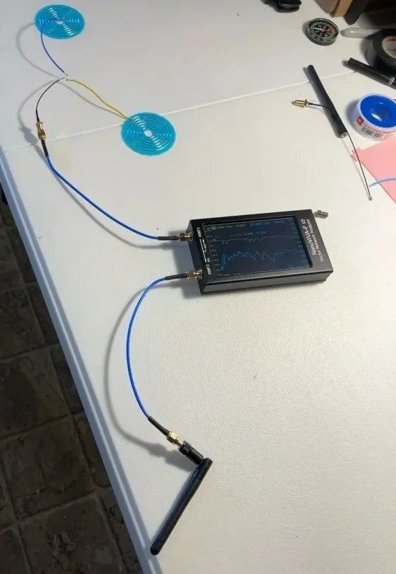
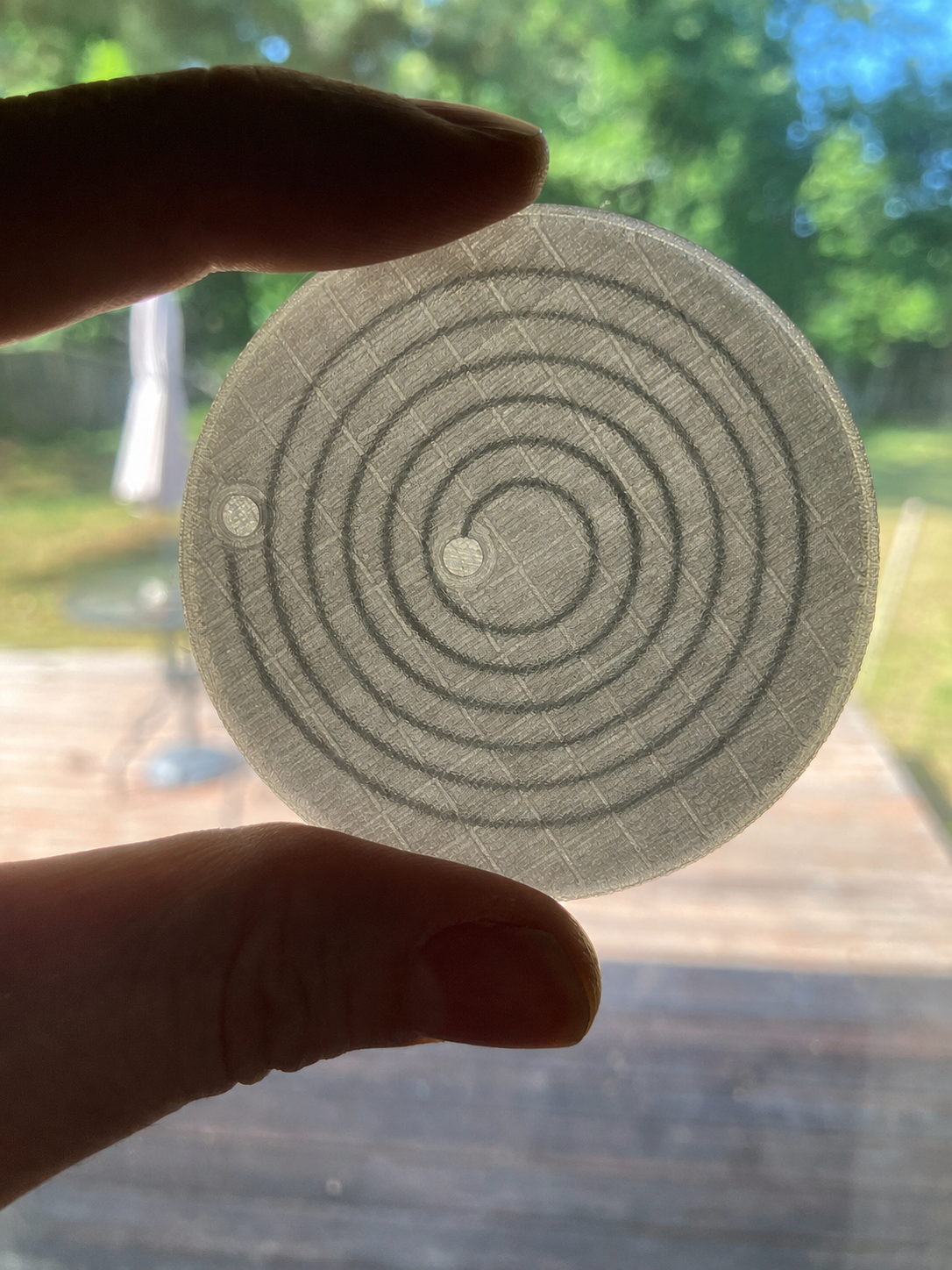
Coils and inductors
Electronic components
Solderable interfaces
Grounding and shielding features
This allows electrical functionality to be designed into the part from the beginning rather than added after printing.
Kupros has already demonstrated the integration of electronic components and conductive features directly within FDM/FFF printed structures.
Electronic Components Embedded During the Print
The process is not limited to printing conductive traces.
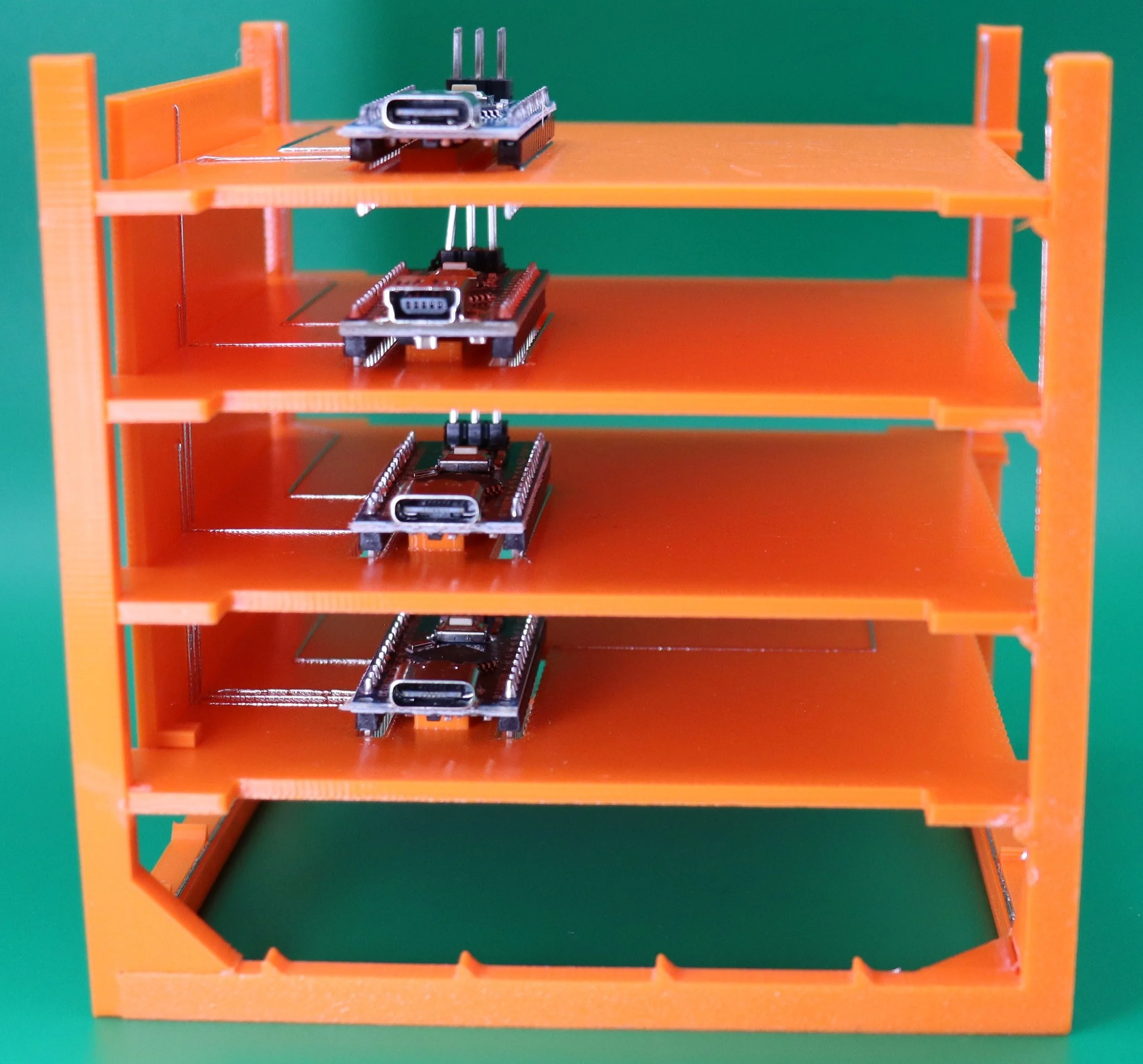
Discrete electronic components can be introduced directly into the FDM/FFF manufacturing workflow and electrically connected using printed Cu29 conductive features.
Depending on the application, this can include components such as:
Resistors
Capacitors
LEDs
Sensors
Passive electronic components
Electrical interfaces
Other discrete electronic devices
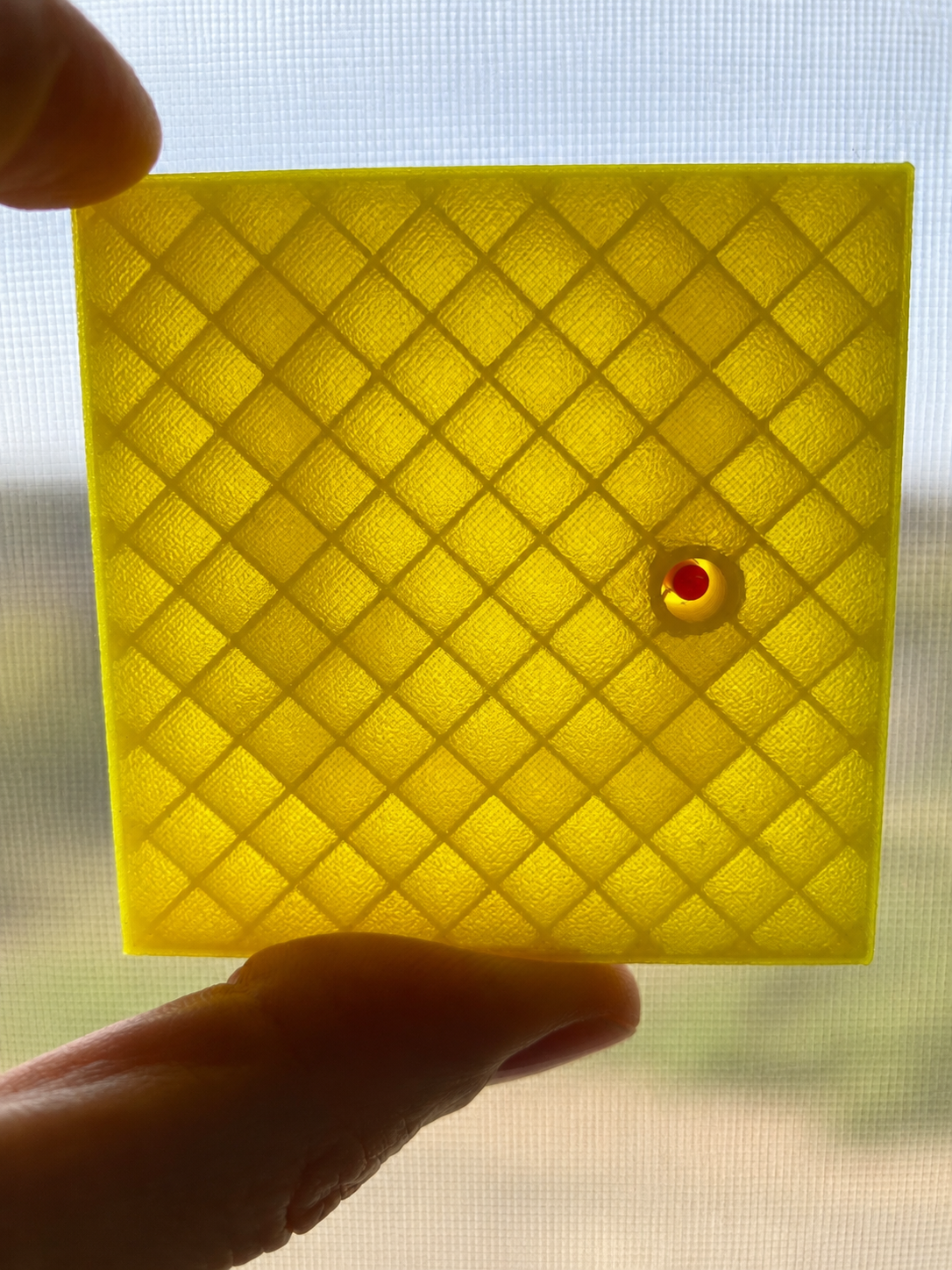
Kupros has demonstrated functional embedded circuits where the polymer structure, conductive pathways and electronic components are integrated during the print workflow.
The goal is straightforward:
A functional electronic assembly directly from the 3D printing process, without having to build the mechanical part first and install the electronics afterward.
3D Printed Embedded Circuits
Traditional electronics manufacturing is largely based around flat circuit boards connected to the surrounding structure through wiring, connectors and mechanical hardware.
FDM embedded electronics remove that geometric restriction.
Conductive pathways can be routed:
Across surfaces
Through internal layers
Around curves
Between different levels of a structure
Around mechanical features
Directly to embedded components
Through complex three-dimensional geometries
This makes it possible to develop electronic systems that follow the geometry of the product rather than forcing the product to accommodate a flat PCB.
Embedded Sensors
Sensors can be incorporated directly into 3D printed structures rather than mounted onto the completed part.
Kupros is developing embedded and surface-integrated sensor architectures including:
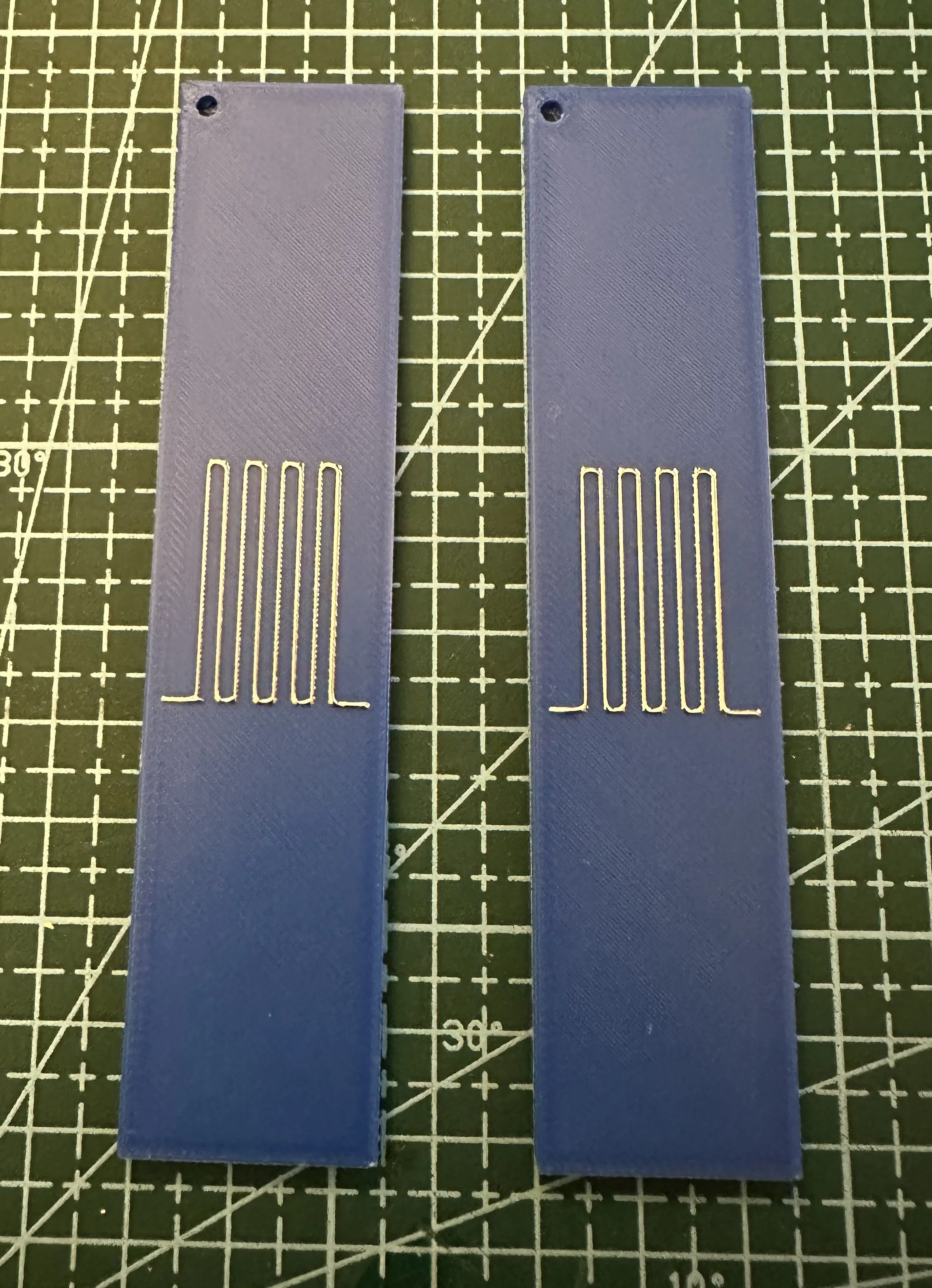
Strain gauges
Structural health monitoring
Resistive sensing
Conductive sensing features
Flexible sensors
Embedded diagnostic pathways
The sensor, conductor and supporting structure can all become part of the same additive manufacturing design.
Embedded Antennas and RF Structures
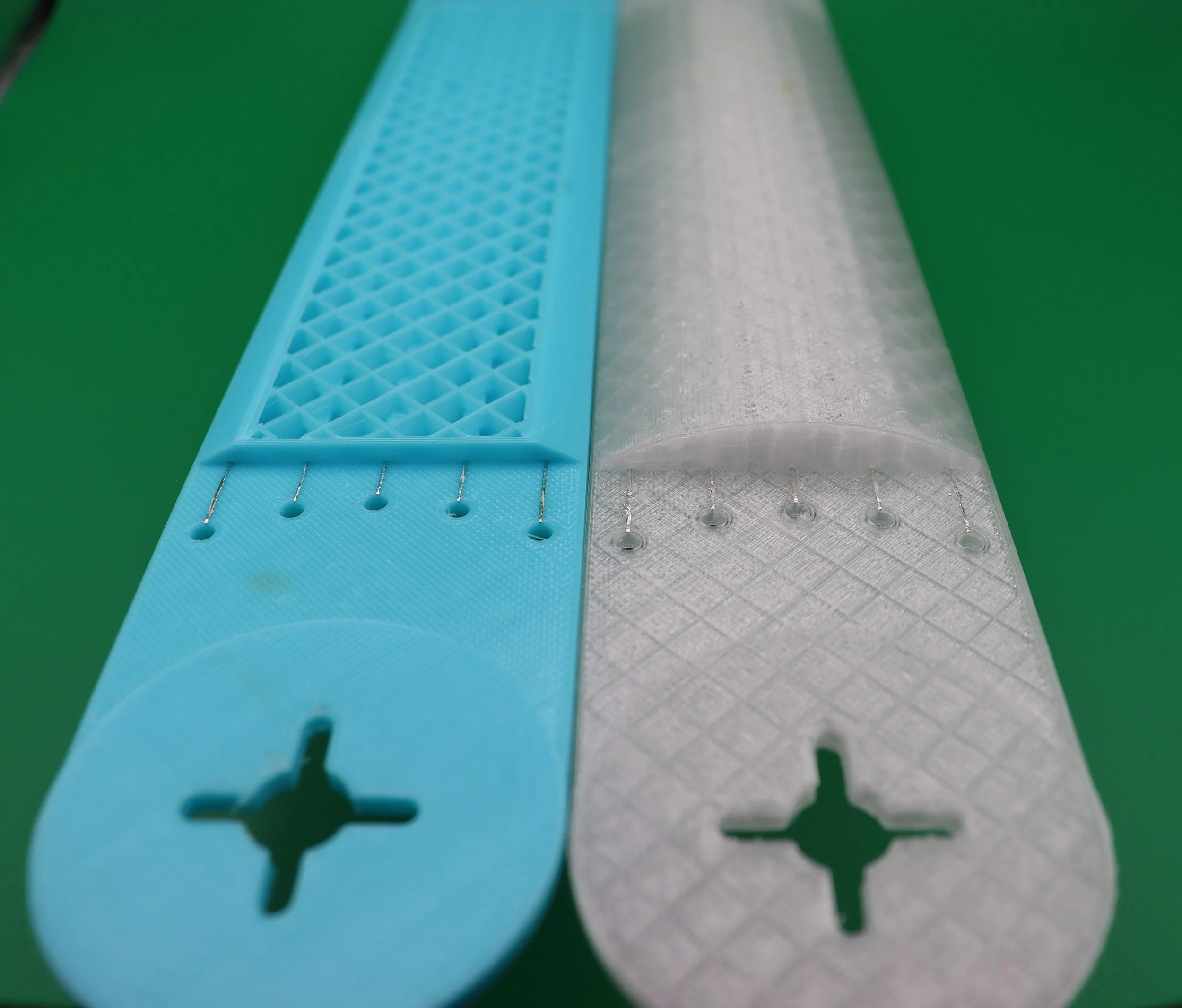
Cu29 also enables conductive antenna and RF geometries to be printed directly into or onto FDM/FFF structures.
Potential applications include:
Conformal antennas
Embedded antennas
Dipole antenna structures
RF features
Conductive coils
Grounding structures
EMI and RF shielding
Three-dimensional RF geometries
Rather than attaching a separate antenna after manufacturing, the antenna can be designed as part of the structure itself.
All-Metal Conductive Pathways with Cu29
The embedded electronics process is enabled by Kupros Cu29, our all-metal, conductive filament for standard FDM/FFF printers.
Cu29 does not rely on a polymer binder in the conductive pathway.
It also does not require:
Sintering
Plating
Curing
Chemical processing
Binder removal
Conductive Cu29 features are electrically functional directly after printing.
Published resistivity: 1.226 × 10⁻⁵ Ω·cm
Cu29 works across FDM/FFF equipment ranging from desktop printers costing less than $400 to industrial systems costing more than $250,000.
Embedded Electronics Beyond Standard Polymers
Kupros' patent-pending embedded electronics architecture is designed around material-extrusion manufacturing rather than one specific polymer.
That creates a path toward integrating electronic functionality into a much broader range of printable materials, including:
Engineering thermoplastics
High-performance polymers
Flexible materials
Composite materials
Ceramic and ceramic-compatible systems
Specialty and exotic FDM/FFF materials
Material compatibility, processing conditions and electronic integration requirements depend on the specific application.
This is especially important for aerospace, defense, space and advanced manufacturing programs where the surrounding structure may require far more than a standard consumer thermoplastic.
Why Embed Electronics During Manufacturing?
Every wire, connector, circuit board, fastener and secondary assembly step adds something to a system.
Weight.
Volume.
Labor.
Failure points.
Lead time.
Embedded electronics create another option.
Instead of designing a mechanical structure around an electronics package, engineers can begin designing the mechanical and electrical systems together.
Potential benefits include:
Reduced wiring
Fewer connectors
Lower part count
Reduced assembly
More compact electronics packaging
Faster prototyping
Three-dimensional electrical routing
Conformal electronics
Distributed electronics
Greater design freedom
Point-of-need manufacturing
For some applications, the best circuit board may eventually be no separate circuit board at all.
From Prototype to Functional Electronics
Kupros is developing embedded electronics workflows for applications across:
Aerospace and Space
Embedded wiring, antennas, sensors, CubeSat structures, RF features and compact electronic assemblies.
Defense and UAS
Embedded power distribution, antennas, sensors, shielding, payload electronics and mission-specific systems.
Robotics and Autonomous Systems
Integrated sensing, wiring, power pathways and distributed electronics.
Research and Advanced Manufacturing
Rapid development of new circuit geometries, sensors, antennas and multifunctional structures.
Distributed and Point-of-Need Manufacturing
Produce electronically functional components using existing FDM/FFF infrastructure rather than relying exclusively on centralized electronics fabrication.
Patent-Pending FDM/FFF Embedded Electronics Process
Kupros has filed patent-pending intellectual property covering the integration of all-metal conductive filaments, conductive pathways and electronic components within FDM/FFF additive manufacturing workflows.
The process expands Kupros beyond conductive filament alone.
We are developing the materials and manufacturing methods required to produce structure and electronic functionality together.
Cu29 provides the conductor.
FDM/FFF provides the manufacturing platform.
Embedded component integration turns the printer into something much more capable.
An electronics manufacturing platform.
See Embedded Electronics in Action
Kupros has demonstrated multiple FDM/FFF electronic structures including:
Embedded LED circuits
Embedded resistors
Embedded induction coils
Flexible electronics
Printed conductive pathways
Embedded wiring
Sensors and strain gauges
Antenna structures
Solderable electronic interfaces
[View Cu29 Applications]
Develop an Embedded Electronics Application with Kupros
If your organization is developing a circuit, sensor, antenna, power pathway, electronic enclosure or multifunctional structure that could benefit from embedded electronics, Kupros can help evaluate the application.
We work with organizations across defense, aerospace, space, national laboratories, universities, research and advanced manufacturing.
Contact Kupros to discuss your embedded electronics application.
[Request an Embedded Electronics Evaluation]
Cu29 materials, technical data and support may be subject to U.S. export-control requirements.