
Conductive 3D Printing: Ink vs Filament
Conductive 3D printing enables electrical functionality to be built directly into manufactured components. This article compares conductive ink systems and conductive filament approaches.
Conductive materials are what make conductive 3D printing possible. Instead of fabricating circuits separately and mounting them onto structures later, conductive printing technologies allow electrical features to be produced directly during the manufacturing process.
This capability sits within the broader category of 3D printed electronics, where circuits, antennas, and sensors are integrated into the physical structure of a component rather than assembled afterward.
Conductive Ink Printing
Many additive electronics systems rely on conductive inks that contain metallic nanoparticles, most commonly silver. These inks are deposited onto substrates using inkjet or aerosol printing systems to create electrical traces.
After printing, the traces typically require additional processing steps such as curing or sintering to achieve usable electrical conductivity. These extra steps can introduce workflow complexity and require tightly controlled processing conditions.
Ink-based approaches are often used when extremely fine traces are required or when working with specialized additive electronics machines designed for high-resolution deposition.
Conductive Filament Printing
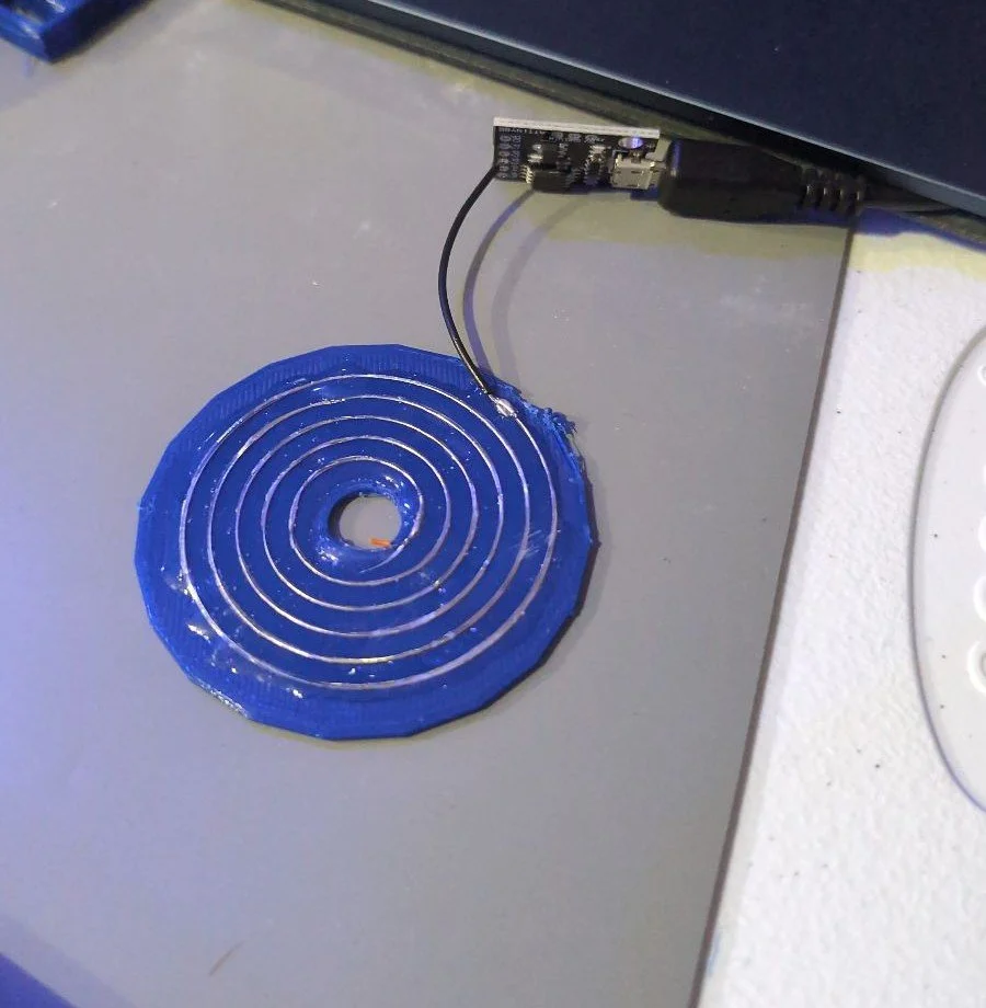
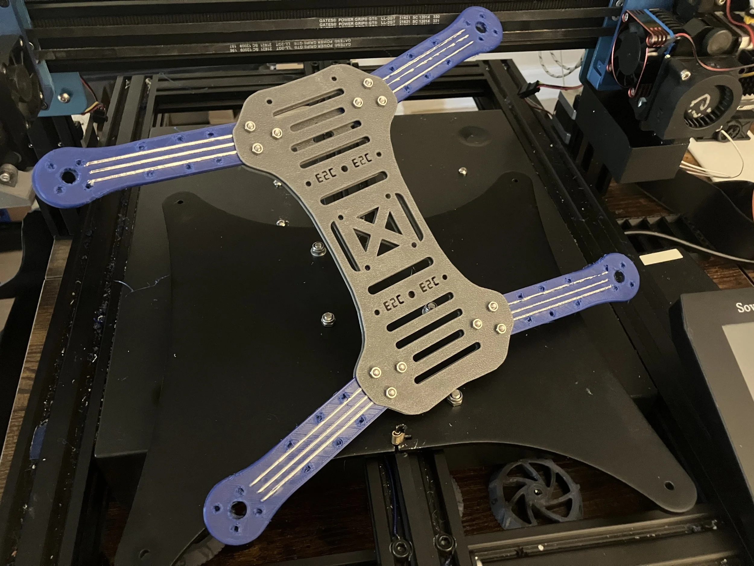
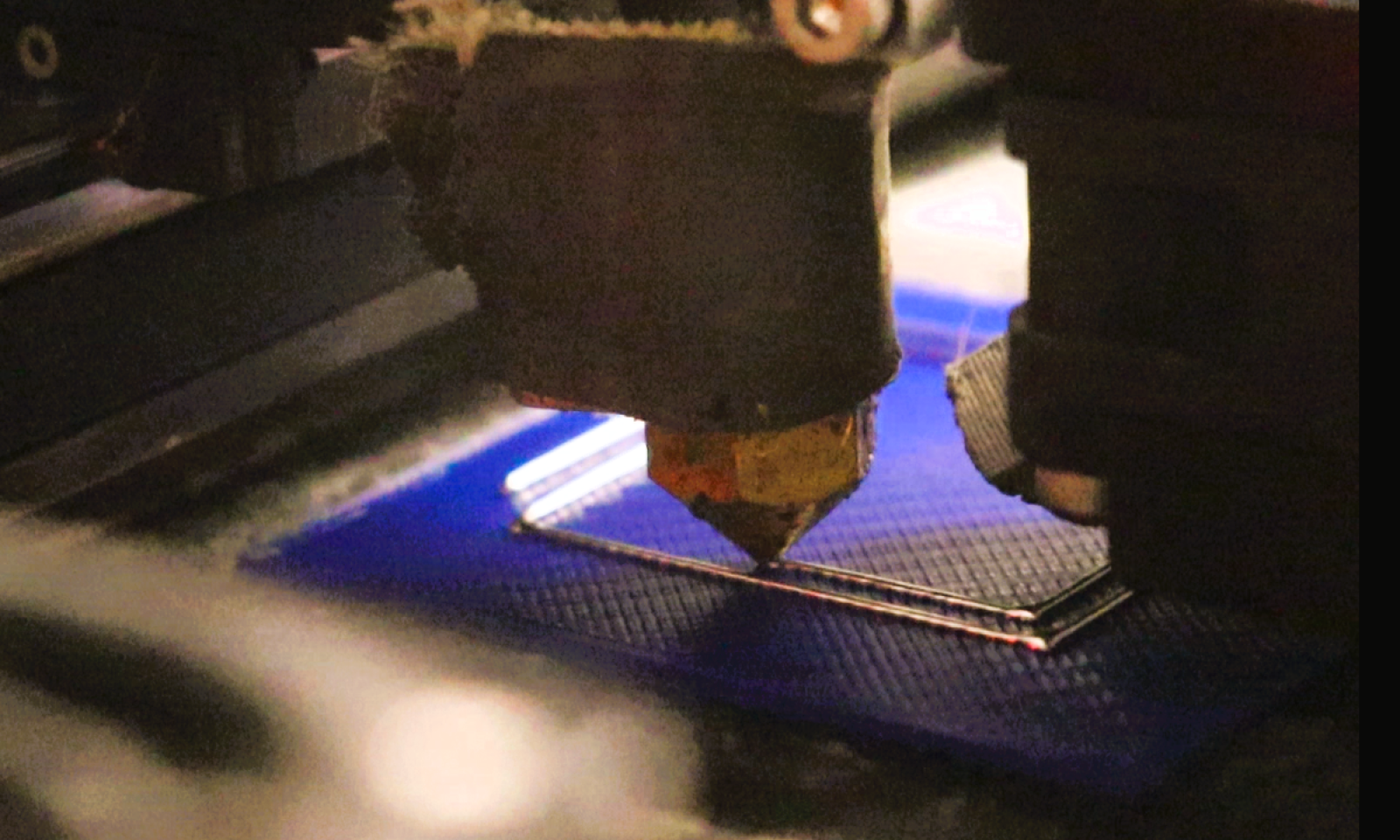
An alternative approach uses conductive filament in FDM or FFF 3D printers. Instead of depositing conductive material onto a surface, conductive filament is extruded through the printer nozzle and integrated directly into the printed part.
This method allows electrical pathways to be printed alongside structural materials within the same component. Conductive filament workflows enable electrical and mechanical features to be manufactured simultaneously.
Examples of what conductive filament printing can enable include:
Embedded signal routing
Integrated sensors
Conformal conductive paths
Embedded antennas
Multi-material printed electronics
Embedded 3D Printed Electronics
One of the most significant advantages of filament-based systems is the ability to create embedded 3D printed electronics. Instead of mounting electronics after a component is manufactured, conductive features can be printed directly into the structure itself.
This approach enables engineers to design mechanical and electrical systems together instead of treating them as separate assemblies.
Embedded conductive pathways can reduce wiring harnesses, simplify assembly, and allow electrical routing to follow complex geometries that would be difficult to achieve with traditional planar circuit boards.
Comparing Ink and Filament Approaches
Both conductive inks and conductive filament systems play important roles in additive electronics. However, they are optimized for different engineering goals.
Ink-based systems often prioritize resolution and precision, making them useful for micro-scale traces and research applications.
Filament-based systems emphasize integration and structural embedding, allowing electrical functionality to be incorporated directly into printed parts.
For many applications involving embedded electronics, the ability to integrate conductors directly into structural components can simplify system architecture and accelerate development.
Where Conductive 3D Printing Fits
Conductive additive manufacturing expands the design space available to engineers. Instead of relying exclusively on planar boards, electrical features can be integrated directly into mechanical components.
This approach is particularly valuable when geometry, integration, or rapid iteration are key drivers in system design.
Organizations evaluating conductive additive manufacturing often begin by building a small subsystem prototype to determine where embedded electrical features provide practical advantages.
Embedded Electronics for Aerospace and Defense Applications
Embedded electronics integrate electrical functionality directly into structural components. This article explores how embedded 3D printed electronics apply to aerospace and defense systems.e
Modern aerospace and defense systems demand lighter structures, fewer components, and faster development cycles. One emerging solution is embedded electronics, where electrical functionality is integrated directly into structural components instead of being mounted afterward.
This approach is increasingly enabled by 3D printed electronics, which allow conductive features such as circuits, antennas, and sensors to be manufactured directly into complex geometries.
Why Embedded Electronics Matter
Traditional electronics architecture often requires separate circuit boards, wiring harnesses, connectors, and mounting structures. These additional components increase system weight, introduce failure points, and complicate assembly.
Embedded electronics allow designers to integrate conductive pathways directly into the physical structure of a component. This integration can reduce part counts, simplify routing, and improve overall system efficiency.
For aerospace and defense platforms where weight, reliability, and space are critical constraints, embedded integration offers clear advantages.
Embedded Antennas and RF Structures
One particularly valuable application of embedded electronics is the integration of RF antennas directly into structural components.
Traditional antennas are typically mounted externally or attached to circuit boards. Embedded manufacturing approaches allow antennas to be printed directly into surfaces or internal structures, enabling conformal antenna geometries that follow the shape of the platform.
This capability can improve aerodynamics, reduce external components, and enable more flexible system architectures.
Sensors and Structural Electronics
Embedded electronics also allow sensors to be integrated directly into mechanical components. Instead of attaching sensors after manufacturing, conductive pathways and sensing elements can be printed directly into the structure.
This enables new approaches to monitoring structural health, environmental conditions, or system performance without increasing assembly complexity.
The ability to embed sensing capability within structural components is particularly valuable in aerospace systems where access and maintenance can be challenging.
Embedded Electronics with Conductive Filament
Additive manufacturing approaches using conductive filament allow electrical pathways to be printed alongside structural materials within the same part.
Instead of producing electronics separately and assembling them later, conductive filament systems enable electrical functionality to be built directly into the manufacturing process.
This method supports the development of:
Embedded antennas
Integrated sensors
Conformal conductive routing
Multi-material structural electronics
Embedded 3D Printed Electronics in Development Workflows
For aerospace and defense engineering teams, one of the biggest advantages of embedded 3D printed electronics is faster development cycles.
Traditional electronics manufacturing requires separate design and fabrication processes for mechanical and electrical systems. Embedded additive approaches allow both systems to evolve together during design.
This integration can significantly reduce iteration cycles when developing complex platforms or experimental subsystems.
Where Embedded Electronics Fit
Embedded electronics will not replace traditional PCB manufacturing in every application. High-density circuit boards remain essential for many electronic systems.
However, embedded approaches provide new options when geometry, integration, or system complexity create limitations for conventional architectures.
Organizations exploring embedded electronics often begin with a subsystem evaluation to determine where integrated conductive features can reduce complexity or improve performance.
What Is Additive Manufactured Electronics (AME)?
Additive Manufactured Electronics (AME) uses additive processes to create circuits on or within structures. This article explains how AME works, its limits, and where embedded 3D printed electronics fits.
Additive Manufactured Electronics (AME) is the process of building electronic circuits using additive manufacturing methods instead of traditional subtractive PCB fabrication. In practical terms, AME is part of the broader category of 3D printed electronics, where conductive features are printed onto or into a substrate rather than etched from copper-clad boards.
How AME Works
Most AME workflows use one of three approaches:
Ink-based deposition of conductive materials
Hybrid systems that print dielectric and conductive layers
FDM-based approaches using conductive filament
Ink-based approaches often print metallic nanoparticle inks and then require curing or sintering to reach useful conductivity. Hybrid systems build multi-layer stacks through multiple print and deposition steps. FDM-based approaches use conductive filament to print conductive paths directly as part of the build.
What AME Solves
AME is useful when you need rapid iteration without committing to tooling or minimum order quantities. It can also enable embedded electronics integration when the goal is to place conductive paths, sensors, or RF features directly into the structure instead of mounting electronics afterward.
Where AME Is Limited
AME is not a universal replacement for traditional PCBs. Many AME systems require specialized equipment and controlled processes, and some approaches are constrained by post-processing steps, substrate compatibility, and current-carrying capability.
Traditional PCB fabrication remains the best tool when you need high-density, high-speed planar routing at volume. AME becomes compelling when geometry, iteration speed, and integration outweigh the advantages of a conventional board.
Embedded AME Using Conductive Filament
One branch of AME focuses on embedded conductors using conductive filament in FDM systems. Instead of printing traces on a flat board, conductive features can be printed into the part itself.
This can enable:
Embedded signal routing
Integrated sensors
Conformal conductive paths
Embedded antennas and RF structures
AME and Embedded 3D Printed Electronics for Aerospace and Defense
Aerospace and defense systems often benefit from embedded 3D printed electronics because geometry, weight, assembly complexity, and iteration speed are operational constraints, not edge cases.
When electronics can be embedded into structure, teams can reduce interconnects, simplify routing, and prototype faster without waiting on external fabrication cycles for every iteration.
Where AME Fits in Modern Manufacturing
AME expands the design space. It does not erase PCBs.
The practical model is hybrid:
Use PCBs when planar density and production scale dominate
Use AME when integration, geometry, and iteration speed dominate
If you want to evaluate AME without overcommitting, the fastest path is to start with a subsystem evaluation where wiring, geometry, or iteration speed is already causing pain.
3D Printed Electronics vs Traditional PCB Manufacturing
Traditional PCB manufacturing is optimized for scale and planar design. 3D printed electronics introduces embedded integration, rapid iteration, and geometric freedom. Here is where each approach wins.ll Begins Here
For decades, electronics have been built the same way.
Design the circuit. Send the files out. Wait for the boards. Assemble. Test. Redesign. Repeat.
Traditional printed circuit boards are reliable and mature. But they are also rigid, planar, and tied to procurement cycles that dictate engineering speed.
As systems become more integrated and schedule-compressed, engineers are starting to evaluate whether flat boards are always the right answer. This is where 3D printed electronics enters the conversation.
The PCB Model: Mature, Planar, Procurement-Driven
Traditional PCB manufacturing is optimized for scale.
Copper is laminated onto substrate. Unwanted material is etched away. Layers are stacked, drilled, plated, masked, and finished. When a design is finalized and volume is high, this model is extremely efficient.
But the constraints are structural:
Circuits must remain planar
Complex geometry requires separate mechanical assemblies
Wiring harnesses add weight and failure points
Iteration is tied to supplier lead times
If a design changes mid-cycle, the delay is not just technical. It is procedural.
This works well when a design is stable and high-volume production justifies setup costs. It is less efficient when development speed and geometry flexibility matter more than scale.
Iteration Speed Changes the Equation
The most expensive board is often the one you are waiting for.
When prototyping requires multiple external fabrication cycles, engineering speed slows to match vendor throughput. Even fast-turn PCB services still require queueing, fabrication, inspection, and shipping.
Additive approaches compress that loop.
With 3D printed electronics, functional prototypes can be produced in hours, not weeks. The geometry can evolve with the mechanical design. Conductive paths can be adjusted and reprinted immediately.
That shift is not about replacing every PCB. It is about removing iteration latency during the phase where design freedom matters most.
Geometry Is the Real Constraint
PCBs are fundamentally flat.
If your system requires curvature, conformal routing, or embedded sensing inside structure, you compensate with brackets, fasteners, adhesives, and interconnects.
Each additional interface introduces mass, complexity, and potential failure points.
3D printed electronics removes the planar assumption.
Conductive paths can follow structural geometry. Sensors can be embedded directly inside printed housings. Antennas can be integrated into load-bearing components instead of mounted afterward.
That is not aesthetic. It is architectural.
Conductivity and Post-Processing Matter
Early additive electronics systems relied heavily on conductive inks. Those systems can produce fine features, but they typically require post-processing steps such as curing or sintering to achieve useful conductivity.
Post-processing adds equipment requirements, thermal constraints, and workflow complexity.
Power-grade embedded systems require something different.
High-conductivity conductive filaments designed for FDM platforms eliminate secondary curing steps and enable conductive traces to be printed as part of the build process.
That simplifies integration and reduces handling variables.
Cost Is Phase-Dependent
Traditional PCBs dominate high-volume production. Once tooling and setup are amortized, per-unit cost is extremely competitive.
3D printed electronics is strongest earlier in the lifecycle:
Prototyping
Low-volume specialty builds
Complex geometry integration
On-demand subsystem manufacturing
Eliminating tooling, minimum order quantities, and external fabrication cycles changes the economics of development.
It does not replace mass production PCB lines. It complements them.
Where Each Technology Wins
Traditional PCB manufacturing is strongest when:
The design is stable
Geometry is planar
Production volume is high
3D printed electronics is strongest when:
Rapid iteration is critical
Geometry is complex or conformal
In-house control improves schedule
For aerospace, defense, and advanced manufacturing systems, the advantage is often not just electrical. It is structural and logistical.
The Practical Approach
This is not a binary decision.
Most advanced engineering teams will use both.
Traditional PCBs for finalized, high-volume electronics.
3D printed electronics for rapid development, structural integration, and embedded functionality.
If you are evaluating whether embedded 3D printed electronics can reduce design cycles or remove mechanical constraints in your system, start with a constrained subsystem and test the architecture.